

Researcher Yang Liang's research group at the Suzhou Institute for Advanced Study at the University of Science and Technology of China developed a new method for metal oxide semiconductor laser micro-nano manufacturing, which realized the laser printing of ZnO semiconductor structures with submicron precision, and combined it with metal laser printing , for the first time verified the integrated laser direct writing of microelectronic components and circuits such as diodes, triodes, memristors and encryption circuits, thus extending the application scenarios of laser micro-nano processing to the field of microelectronics, in flexible electronics, advanced sensors, Intelligent MEMS and other fields have important application prospects. The research results were recently published in "Nature Communications" under the title "Laser Printed Microelectronics".
Printed electronics is an emerging technology that uses printing methods to manufacture electronic products. It meets the characteristics of flexibility and personalization of the new generation of electronic products, and will bring a new technological revolution to the microelectronics industry. Over the past 20 years, inkjet printing, laser-induced transfer (LIFT), or other printing techniques have made great strides to enable the fabrication of functional organic and inorganic microelectronic devices without the need for a cleanroom environment. However, the typical feature size of the above printing methods is usually on the order of tens of microns, and often requires a high-temperature post-processing process, or relies on a combination of multiple processes to achieve the processing of functional devices. Laser micro-nano processing technology utilizes the nonlinear interaction between laser pulses and materials, and can achieve complex functional structures and additive manufacturing of devices that are difficult to achieve by traditional methods with a precision of <100 nm. However, most of the current laser micro-nano-fabricated structures are single polymer materials or metal materials. The lack of laser direct writing methods for semiconductor materials also makes it difficult to expand the application of laser micro-nano processing technology to the field of microelectronic devices.
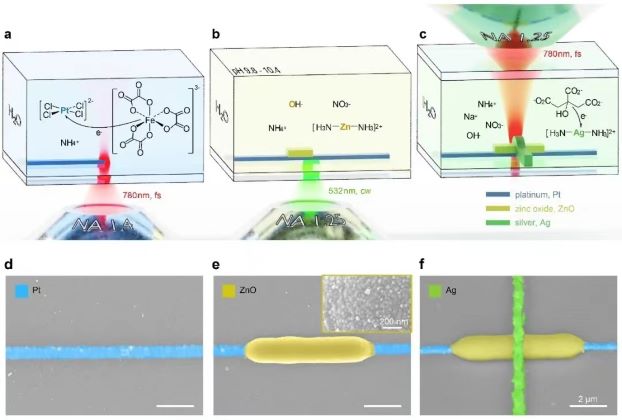
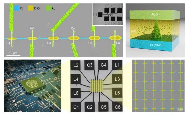
In this thesis, researcher Yang Liang, in cooperation with researchers in Germany and Australia, innovatively developed laser printing as a printing technology for functional electronic devices, realizing semiconductor (ZnO) and conductor ( Composite laser printing of various materials such as Pt and Ag) (Figure 1), and does not require any high-temperature post-processing process steps at all, and the minimum feature size is <1 µm. This breakthrough makes it possible to customize the design and printing of conductors, semiconductors, and even the layout of insulating materials according to the functions of microelectronic devices, which greatly improves the accuracy, flexibility, and controllability of printing microelectronic devices. On this basis, the research team successfully realized the integrated laser direct writing of diodes, memristors and physically non-reproducible encryption circuits (Figure 2). This technology is compatible with traditional inkjet printing and other technologies, and is expected to be extended to the printing of various P-type and N-type semiconductor metal oxide materials, providing a systematic new method for the processing of complex, large-scale, three-dimensional functional microelectronic devices.
Thesis :https://www.nature.com/articles/s41467-023-36722-7
Post time: Mar-09-2023